Capability of Rigid board |
||
No. |
Type |
Standard |
1 |
Normal FR4/Halogen free/ |
KB,Shengyi, ITEQ,Isola, |
2 |
PTFE Laminates |
Rogers series、Taconic series、 |
3 |
Hybrid laminating |
Rogers/Taconic/Arlon/Nelco |
4 |
Multilayers |
4-64 layers, board thickness |
5 |
Buried/Blind Via |
4-50 layers, |
6 |
HDI |
1+N+1、2+N+2、 |
7 |
Flex & Rigid-Flex PCB |
1-12layers Flex PCB ,2-20layers |
8 |
Soldermask Type(LPI)/ |
kuangshun,Taiyo、 |
9 |
Peelable Soldermask/color |
PETER SD2955/Blue-Green |
10 |
Carbon ink |
Nipon |
11 |
HASL/Lead Free HASL |
Thickness: 0.5-40um |
12 |
OSP |
Entek Plus HT, Preflux F2 LX |
13 |
ENIG (Ni-Au) |
Au:0.03um≤max<0.06um |
14 |
Electro-bondable Ni-Au |
Au:0.2-1.0um Ni:2.54-10um |
15 |
ENEIPG |
Au: 0.015-0.075um |
16 |
Electro. Hard Gold |
Au:5~50uin(0.125~1.27um); |
17 |
Thick tin |
1.0-1.4um |
18 |
Copper thickness |
12oz max. |
19 |
Min Mechanical Drill Hole |
0.15mm |
20 |
Min. Laser Drill Hole |
4mil (0.100mm) |
21 |
Line Width/Spacing |
2mil/2mil |
22 |
Max. Panel Size |
650mm X 1200mm |
23 |
Line Width/ |
Non electro coating:+/-5um, |
24 |
PTH Hole Tolerance |
+/-0.002inch(0.050mm) |
25 |
NPTH Hole Tolerance |
+/-0.002inch(0.050mm) |
26 |
Hole Location Tolerance |
+/-0.002inch(0.050mm) |
27 |
Hole to Edge Tolerance |
+/-0.004inch(0.100mm) |
28 |
Edge to Edge Tolerance |
+/-0.004inch(0.100mm) |
29 |
Layer to Layer Tolerance |
+/-0.003inch(0.075mm) |
30 |
Impedance Tolerance |
+/- 10% /Max >50ohm +/- 5% |
31 |
Warpage % |
Max ≤0.5% |
Capability of Rigid-flex board |
||
NO. |
Item |
Standard |
1 |
Flex & Rigid-Flex PCB |
1-30layers Flex PCB , |
2 |
FCCL(adhesive) |
Shengyi SF305:PI= |
3 |
FCCL(adhesiveless) |
Panasonic R‐F775(ER): |
DuPont Pyralux |
||
4 |
Coverlay |
Shengyi SF305C: 0515& |
Taiflex FHK: 1025&1035 |
||
5 |
Adhesive |
Taiflex BT: AD=10um& |
shengyi SF302B: |
||
6 |
PI stiffener |
Taiflex MHK: PI=3mil, |
7 |
3M |
9077&6677&9458 |
8 |
NO FLOW PP |
Ventec:VT‐47N(TG 170℃)& |
9 |
CCL |
ITEQ: IT‐180A; |
10 |
Other CCL |
Arlon: 85N; Rogers: |
11 |
Board thickness |
0.3mm‐3.0mm |
12 |
Tolerance of board |
±10% |
13 |
Tolerance of board |
±0.1mm |
14 |
Min. board size |
10mm*15mm |
15 |
Max. board size |
406.4mm*558.8mm |
16 |
Impedance control |
±10% |
17 |
Bow&twist |
0.75%(symmetrical), |
18 |
Min. BGA pad size |
12mil(8mil for electrical |
19 |
Max. finished |
3oz |
20 |
Max. buried via |
0.4mm |
21 |
Tolerance of |
±2mil(limited is +0/‐ |
22 |
Solder mask color |
green,blue,red, matte green, |
23 |
Min. solder dam |
4mil(green, red and blue), |
24 |
Min. solder dam |
8mil |
25 |
Min. clearance |
2.5mil (2.0mil) |
26 |
Surface treatment |
HASL/LF HASL, |
Thickness (ENIG) |
0.05‐0.10um |
|
27 |
Nickel thickness |
3‐8um |
Gold thickness |
0.05‐0.10um |
|
28 |
Palladium thickness |
0.05‐0.15um |
Nickel thickness |
3‐8um |
|
29 |
Hard gold thickness |
0.1‐1.5um |
Hard gold thickness |
0.1‐4.0um |
|
30 |
Electrolytic Nickel |
≥3um |
Electrolytic Gold thickness |
0.05‐0.10um |
|
31 |
Immersion silver thickness |
0.2‐0.4um |
OSP thickness |
0.1‐0.3um |
|
32 |
Tolerance of board outline |
±6mil(exclude complicated |
Manufacturing Processes

- Step 1 -
Customer data pre-audit
- Step 2 -
Sales offer
- Step 3 -
Engineering data production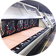
- Step 4 -
Cutting, drilling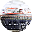
- Step 5 -
Graphics transfer
- Step 6 -
Plating, etching
- Step 7 -
Solder mask, text
- Step 8 -
Surface treatment process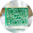
- Step 9 -
Forming
- Step 10 -
Detection
- Step 11 -
Shipment